Connected PCB Design with Autodesk Product Design & Manufacturing Collection


Connected PCB Design with Autodesk Product Design & Manufacturing Collection
Revolutionising Electronics Design: How Autodesk Inventor's PCB Interoperability Tools are Changing the Game
Autodesk Inventor is a powerful CAD software that offers a range of advanced features for mechanical and electrical design. One of the most valuable features for electronic designers is the ability to work with printed circuit boards (PCBs) directly in the software. With Autodesk Inventor’s PCB interoperability tools, users can streamline their design process and create more accurate designs
How to Achieve Connected Design with Autodesk Inventor and Eagle (Fusion 360)
Are you looking to streamline your printed circuit board (PCB) design workflow? Look no further than Autodesk’s connected design solution between Inventor and Eagle. This powerful combination allows for seamless collaboration between mechanical and electrical design teams. Autodesk Eagle, now a part of Fusion 360, is a popular PCB design tool that offers a range of powerful features to create schematics, layout designs, and manufacturing outputs. By integrating Eagle with Inventor, designers can easily incorporate PCBs into their mechanical assemblies and optimize the fit and function of their designs.
One key advantage of using Inventor and Eagle together is the ability to maintain a “single source of truth” for your design data. With the integration, design changes in one tool can be automatically propagated to the other, reducing the risk of errors and ensuring consistency across the design process.
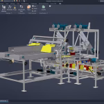
Another benefit of this connected design approach is the ability to visualize the PCB and its components in a 3D mechanical assembly context. This allows designers to check for potential interferences, optimize the placement of the PCB and its components, and ultimately achieve a more efficient and cost-effective design.
To get started with connected design between Inventor and Eagle, simply import your Eagle board file into Inventor. From there, you can place the PCB into your assembly and start working on the integration with your mechanical components. Changes made to the PCB in Eagle will be reflected in Inventor, and vice versa.

Inventor's PCB Interoperability Tools
Inventor offers a suite of tools for working with PCBs, including:
ECAD-MCAD Collaboration
This tool allows electrical and mechanical designers to work together seamlessly by importing 3D models of the PCB into Inventor. This tool eliminates the need for physical prototypes and enables designers to test the fit of the PCB in the mechanical assembly.
PCB layout import
Inventor can import and view PCB layouts from other software tools such as Eagle, Altium, and OrCAD. This feature allows designers to view their designs in a 3D environment and make any necessary changes before finalizing the design.
Design rule checking
Inventor offers a comprehensive design rule checking tool that allows designers to check their PCB designs against a set of predefined rules. This feature ensures that the design meets industry standards and helps identify any potential errors before the manufacturing process.
Export to Manufacturing
Once the design is complete, Inventor can export the PCB design to the manufacturing process. This feature ensures that the design is accurate and ready for production.

Streamlining Design Workflows: Importing and Exporting Data Between Autodesk Inventor and Eagle (Fusion 360)
Importing and exporting data between Autodesk Inventor and Eagle is a critical function for any engineer working on a connected design project. Fortunately, the process is straightforward, thanks to the seamless integration between the two applications.
To import an Eagle board into Inventor, the first step is to create a new board assembly in Inventor. Next, click on the Eagle PCB Import command and select the .brd file. Inventor will then import all the PCB data, including the component placement and board outline.
Exporting data from Inventor to Eagle is equally easy. Simply open the board assembly in Inventor and select the Eagle PCB Export command. This will generate a .brd file that can be imported into Eagle, complete with all the board data and component placement.
One critical aspect of importing and exporting data between these two applications is ensuring that the design rules and constraints are consistent. Any discrepancies in the design rules can cause significant issues, including board failures or electrical shorts.
Fortunately, Autodesk has developed a comprehensive set of tools to ensure that data is accurately exchanged between Inventor and Eagle. For example, the Eagle board data is automatically translated into the Inventor format, ensuring that all dimensions and placement data are consistent.
Seamless Integration: How Autodesk Inventor and Fusion 360 Work Together for Streamlined PCB Design
Autodesk Inventor and Fusion 360 are both powerful design tools that can be used for a wide range of applications. While Inventor is known for its advanced 3D design capabilities, Fusion 360 is a comprehensive product development platform that allows designers and engineers to work together in a collaborative environment.
One of the ways that Inventor and Fusion 360 work together is through their interoperability with PCB design software. In particular, Fusion 360 includes an integrated PCB design tool called Eagle that can be used to create schematics and layouts for printed circuit boards. By leveraging the power of Eagle and the design capabilities of Inventor and Fusion 360, designers can create complex PCB designs with ease.
One of the key benefits of using Inventor and Fusion 360 for PCB design is the ability to work in a connected design environment. This means that designers can collaborate in real-time with other members of their team, including electrical engineers, mechanical engineers, and other stakeholders. This collaborative approach can help to streamline the design process and reduce errors, ensuring that the final product is of the highest quality.
Another advantage of using Inventor and Fusion 360 for PCB design is the ability to import and export data between the two platforms. This means that designers can easily move between the two tools, leveraging the strengths of each platform as needed. For example, designers can create a 3D model of a PCB in Inventor, then import the data into Fusion 360 to add electrical components and wiring.
To get started with using Inventor and Fusion 360 for PCB design, users should first become familiar with the basic workflows and tools of each platform. They should also explore the various integration points between the two tools, including the ability to import and export data, collaborate in a connected design environment, and use the integrated Eagle PCB design tool within Fusion 360.
Why Use Autodesk Inventor for PCB Design?
Autodesk Inventor’s PCB interoperability tools make it an ideal choice for electronic designers. The ability to work with both mechanical and electrical designs in the same software environment streamlines the design process and eliminates the need for multiple software tools. This feature also enables designers to test the fit of the PCB in the mechanical assembly, reducing the risk of errors and rework.
Additionally, Inventor’s ability to import and view PCB layouts from other software tools enables designers to work with existing designs and make any necessary changes in a 3D environment. This feature saves time and improves accuracy.
Finally, Inventor’s comprehensive design rule checking tool ensures that the design meets industry standards and identifies any potential errors before the manufacturing process. This feature reduces the risk of costly errors and ensures that the design is accurate and ready for production.
Conclusion
In conclusion, the interoperability between Autodesk Inventor and Fusion 360, along with the integrated Eagle PCB design tool, makes these tools an excellent choice for designers and engineers looking to create complex PCB designs. By working together in a connected design environment and leveraging the strengths of each platform, designers can create high-quality PCB designs in a fraction of the time it would take with other tools.
Ready to get your PCB Design Connected?
Discover how Autodesk Product Design & Manufacturing Collection can streamline your workflow, increase productivity, and optimise your design process.
Get up to 20% Off Software or Services!
Contact us to find out how much money you can save on software, training or other services. Fill out the form below, by live chat, phone or email.
P: 1800 490 514 | E: [email protected]

Connected Design with Product Design & Manufacturing Collection
Click a link below to learn more about Connected Design using the Autodesk Product Design & Manufacturing Collection